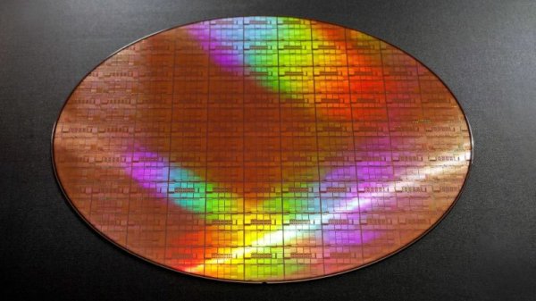
Japan Rapidus trial production 2 nanometer GAA crystal circle, officially mass production in 2027
 According to foreign media reports, Japanese new chip manufacturer Rapidus has started testing production of 2 nanometer crystals and has ordered the IIM-1 factory area volume production target in 2027.
According to reports from
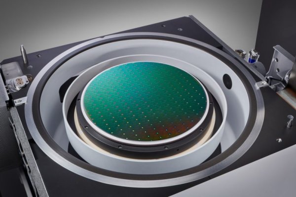
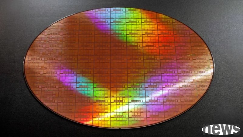
Tom's Hardware, Rapidus Japan IIM-1 factory has started prototyping the test circle using 2-nanometer gate all-ring (GAA) transistor technology. The company confirmed that the early test of the wafer has achieved the expected electric characteristics, which means that its wafer wafer factory tools are operating normally and the process technology is developing smoothly.
Prototyping is an important milestone in semiconductor production, aiming to verify the early test of circuit reliability, efficiency and achieve performance goals made using new technologies. Rapidus is currently measuring the electrical characteristics of its test circuit, including parameters such as boundary voltage, driving current, leakage current, secondary boundary slope, turn-off speed, power consumption and capacitance. Although Rapidus has not announced specific results, it is of great significance to test that the wafer has flowed in the wafer factory.
Rapidus IIM-1 factory has been working normally since September 2023. The dust-free room was completed in 2024. As of June 2025, it has been connected to more than 200 sets of equipment, including advanced DUV and EUV micro-film tools. Rapidus installed advanced EUV tools in December 2024 and successfully made its first exposure in April 2025. At present, the factory has sufficiently mature operation to test the wafer, allowing Rapidus to measure the electrical characteristics of its GAA architecture circuit to identify potential process problems and adjust the settings of the tool or manufacturing step.
Rapidus specifically mentioned that its IIM-1 factory will use the "single round treatment" method for all previous process steps. This is a semiconductor manufacturing method in which each wafer is processed, processed and inspected individually, rather than in combination. Currently, large chip manufacturers such as Intel, Samsung and TECHNOLOGY adopt combinations of combinations and single-dragon processing methods during their semiconductor manufacturing process. Single wafer processing is often used for key steps that require high precision, such as EUV and DUV graphicization, electromechanical etching, atomic layer deposition or defect monitoring. For other steps such as oxidation, ion implantation, cleaning and annealing, they process the wafer in a combined manner.
Rapidus plans to apply the single wafer method to all process steps, including oxidation, ion implantation, graphicization, deposition, etching, cleaning and annealing, etc. Rapidus says this method can accurately control each operation because it can be adjusted according to the conditions or results of a single wafer. Since each wafer is processed independently, engineers can instantly micro-tune parameters, detect abnormalities early, and apply corrections quickly without waiting for the entire combined test to be completed.
In addition, this method produces a larger amount of high resolution data per wafer and can be used to monitor and optimize manufacturing conditions. These algorithms may be able to collect information faster, for continuous process improvement (CPI) to reduce defect density and improve yield, and for statistical process control (SPC) to reduce performance variations. Single-drille processing systems are also easier to change settings and switch between small batches and large production, which is important for Rapidus because its goal is to serve smaller manufacturers.
However, there are some necessary conditions for this method. Due to the processing of the wafer one piece at a time, the production volume (some tools) per tool will be lower than that of large-scale processing, which may extend the production cycle time and increase production costs. This makes the required equipment more complicated and expensive, and the single coordination of the movement of the wafer in all steps increases additional sales. Despite this, Rapidus believes that despite the high upfront costs and slow processing speeds, long-term benefits in reduced defects, improved yields and appropriate process control can make single-dollar processing a powerful strategy for advanced wafer production at 2 nm and more.
To support early customers, Rapidus is preparing to release the first edition of its Process Development Kit (PDK) in the first quarter of 2026, and is also committed to providing customers with the required basic facilities for wafer design prototype production in the IIM-1 factory area.